The core of the B5900 design was the DP-SLC complex, which I modeled after the “Black Box”, the signal processing computer I worked on for my thesis at MIT. The Black Box was a VLW (Very Large Word) processor with a hardware FFT (Fast Fourier Transform) unit and fast local memory. The Black Box processor was designed to interface to a DEC PDP-9 mini-computer, which would feed it high level signal processing operation codes (Op Codes) and data to execute. The Black Box had a control store that was loaded from the PDP-9 which implemented the instruction set.
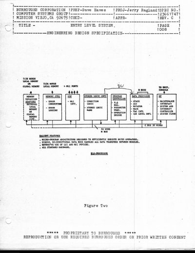
The B5900 worked in a very similar way to the Black Box but was not tied to another computer to obtain its Op Codes. The Program Controller (or PC) was designed to parse the E-mode instructions directly from main memory. The PC would then present the SLC with an entry point to the VLW microcode routine in its memory which corresponded with the desired E-mode instruction. If there were constants or operators with the instruction, the PC would parse those and make them available to the SLC in a standard format. The PC was really the only thing left of the old hardware decode used in the B6XXX series mainframes.
I originally did not pick the name Stored Logic Controller (SLC) for the processor. I picked Microcode Processor. Erv and Ron did not like that name. They were concerned the field support force would be confused. They did not understand the concept of VLW emulation, but the B6800 and B6900 used PROM logic to emulated gates and flip-flops of the B6700. Those computers had a module called the Stored Logic Controller. Now our SLC used static RAM. When the B5900 was powered up the maintenance console read the microcode from an 8” floppy disk and loaded it via the MP into the SLC RAM. If the B5900 lost power, the RAM had to be reloaded; the machine was completely useless without the microcode. Our SLC was a computer, not a simple PROM driven state machine, but I agreed with the name change.
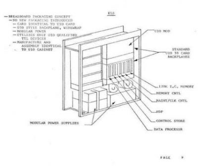
I decided to construct the prototype of the B5900 using what was called a wirewrap breadboard. That was a common technique used in those days to design new computer architectures. The Black Box at MIT was designed as a wirewrap because of the speed and flexibility wirewrap provided. The concept was simple, each IC in the design was placed in a socket on a circuit board that was physically the same as the final design, except instead of the pins being connected by circuit etchings on the surface of the circuit board, they were wired to each other via thin, insulated wires. Each socket had a pin that extended out the back of the circuit board about an inch long. The pins had a square, not round, profile. A person or machine wrapped the bare end of the wire around the pin, and the other end around the proper pin somewhere else on the circuit board, completing the circuit. If a logic error were found in the design, it could be corrected easily. The offending connection was either cut or removed, and a new connection made. Of course, extensive logic errors required more extensive rework, sometimes reworking an entire board. The drawback of a breadboard is that it is not electrically identical to the final design. In the final design the circuit boards would be etched with traces that connected the pins and wires would not be used. Wires and circuit traces have different electrical characteristics. Signals may travel either faster or slower, and you can have something called “crosstalk”, where a signal carried on one trace can radiate into one close by. By the time the B5900 was designed, software programs called simulators were pretty good. Engineers began skipping the breadboard phase and going directly to printed circuits. Errors in design could still creep in, but these were usually fixed with some simple cuts and/or jumper wires. The circuit board with the error could then be “turned”, incorporating the fix before, or shortly after production began (the first several machines may have had these manual fixes). The CTL B6900 was being done this way.
There were really three pragmatic reasons I decided to use wirewrap for the first B5900. As I stated earlier, totally new computer architectures often were prototyped. While the B5900 VLW design was not new to me, it was to Burroughs Mission Viejo, and I felt that if anything were missed, it would be easier to fix. The second was resources; the circuit board group was quite busy designing new circuit boards for the UIO group and the B6900. The UIO circuit board was much larger than those that proceeded it (for example, the B6900 circuit boards were about 4”x5”). Boards were routed using special design automation software that figured out how to connect all the pins, running one UIO board might take 24 hours or more, and sometimes the route failed. When routes failed technicians like Lynn Taylor would attempt to hand route the failed connections. If lots of routes failed then the IC’s would have to be repositioned and the routing tried again. I met with the design automation supervisor and he gave me the skinny, “Jack, we have several hundred B6900 cards to design and route, and we have a lot of UIO work, which is giving us a problem, you submit one of your Data Comm. boards and maybe we can get to it in a month or two, or maybe three?” As an unfunded project, we were the last in the queue, and the queue was pretty long at that time. Finally there was cost, UIO boards were costly to design for the same reasons as above, and we had a very small budget, only $240,000 for the first year.
However, manufacturing’s wirewrap department, whose use was declining in the plant, had an excess of capacity. Wirewrap was used not only for prototypes, but for backplanes, the rows of connectors circuit boards plug into. At this time wirewrap was the main way of wiring backplanes, and manufacturing had large, “Gardner Denver” automated wirewrap machines to wire the backplanes. Early machines, like the B6500 and B6700 had thousands of small circuit cards plugged into several backplanes, so there was a lot of wirewrap work in manufacturing. The B6800 uses about half the number of cards, because the logic was much denser. Instead of a single flip-flop on an IC, you now had four. The B6900 would use even fewer cards because stored logic was much denser. UIO did not use wirewrap at all; it used the modern method of an etched bus backplane. So the factory people were looking for things to do. I went and talked to them about doing the B5900 breadboard, and they were willing to do if for a bargain price. Erv was not totally happy we were going to breadboard the B5900, but he also realized that was about the only way we were going to get one built.
At that time Mission Viejo still did not have design automation for engineers. Graphic workstations were expensive and were in the Design Automation department under Palmer. Design consisted of getting large (B size, 11×14) pieces of paper, and preprinted stick on logic representations of the IC’s, gates, and flip-flops. The engineers stuck them on and drew the connections with pencil. The page then went to design automation where a technician digitized the page. The digitized image was then printed, and from the image a netlist (list of circuit connections) was generated. From that netlist a wirewrap instruction tape could be generated to wire the board.
Because the design automation tools for generating schematics was cumbersome and non-intuitive, I first had each engineer do a block diagram of their part of the B5900. The block diagram is a high-level depiction of the design. For example, the B5900 had thirteen 2901 chips, but functionally they formed a single block, the data path. We used block diagrams to “debug” the specification for the machine. This also pointed out where there were problems. I had two major kinds of problems, some were logic, but the more serious was the ability of my designers.